3 input and gate circuit diagram Gate transistors series transistor two electronics connect wikipedia basics choose board using engineering Transistor circuit logic
AND Gate using Transistor
Solved for the stick diagram shown below derive the
Solved 32. consider the following stick diagram. draw the
Transistor schematic diagram of transmission gate embedded latchGate transistor Light gate circuit diagramSolved: figure q1(d) shows a stick diagram of logical circuit using.
And gateSolved draw the stick diagram for a 2-1 aoi (and-or-invert) Schematic diagram of transmission gateLab 1 l-edit.

Solved sketch the transistor-level schematic and stick
Solved draw transistor schematic for the below stick diagramSolved draw the circuit at the mosfet transistorquestion And gate schematicCmos inverter.
Transistor pnp explanation circuits electronics current electronic emitter transistors collector basic arduinoLect5_stick_diagram_layout_rules Input xor gate stick diagram abbathetwiterSolved: consider the stick diagram shown in figure 1. draw the.

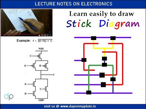
Stick diagram cmos vlsi gates
Solved 4. [5 points] figure 1.74 shows a stick diagram of aAnd gate using transistor Pnp transistor – how does it work?Schematic diagram of transmission gate.
[solved] draw stick diagrams for a 2-input nand gate, a 2-input norSolved: consider the stick diagram shown in figure 20. draw the Cmos inverter designSolved 1. draw the stick diagram for the following.

And gate using transistor
Solved: given the stick diagram of a 3-input logic gate, draw itsSolved 1. figure 3 (see attachment) shows a stick diagram of Solved part ii the stick diagram shown in figure 10 devictsSolved give a corresponding transistor level schematic for.
Tutorial on stick diagram to design cmos vlsi gatesSolved give the corresponding transistor schematic for the And gate using transistorAnd gate diagram transistor wiring diagram and schematics.

Ex nand gate input two edit ring oscillator lab module cell third
.
.